_edited_edit.png)
The transistor is a semiconductor device used to amplify or switch electronic signals and electrical power. It is composed of semiconductor material usually with at least three terminals for connection to an external circuit. A voltage or current applied to one pair of the transistor's terminals controls the current through another pair of terminals. Because the controlled (output) power can be higher than the controlling (input) power, a transistor can amplify a signal.

Types of Transistor

Bipolar Junction Transistor (BJT)
Field Effect Transistor (FET)
Bipolar Junction Transistor

A bipolar junction transistor is a type of semiconductor that uses both electrons and holes as majority carriers. It is the short form of Bipolar Junction Transistor, it is a solid-state current-controlled a device which can be used to electronically switch a circuit, you can think of it as your normal Fan or Light switch, but instead of you turning it on manually it can be controlled electronically. Technically speaking, BJT is a three-terminal device with an Emitter, collector, and a base pin, the current flow through the emitter and collector are controlled by the amount of current applied to the base. Again you can think of emitter and collector as the two ends of your switch and instead of pressing the switch, we have the base pin which can receive the control signal.
Construction of BJT

Explanation The construction can simply be explained with a two diode analogy for transistor as shown in the above image. Consider the two diodes connected with each other using the cathode, then the meeting point can be extended to form the base terminal and the two anodes end acts as the collector and emitter of a PNP transistor. Similarly, if you connect the anode ends of the Diode then the meeting point of the anodes can be extended to for the base terminal and the two cathode ends act as the collector and emitter of the NPN transistor.
Characteristics of a BJT
BJT can be connected in three different configurations by keeping one terminal common and using the other two terminals for the input and output. These three types of configurations respond differently to the input signal applied to the circuit because of the static characteristics of the BJT. The three different configurations of BJT are listed below.
Common Base (CB) configuration
Common Emitter (CE) configuration
Common Collector (CC) Configuration
Among these, The common Base configurations will have voltage gain, but no current gain, whereas the Common Collector configuration has current gain, but no voltage gain and the Common Emitter configuration will have both current and voltage gain.
Symbols of BJT Transistors
The below diagram shows the symbols of the two types of transistors. The one on the left is the symbol of the PNP transistor and the one on the right is the symbol of the NPN transistor.
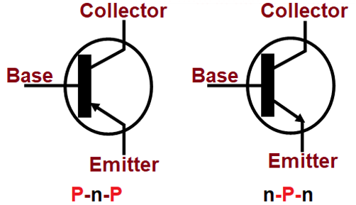
Difference Between P-n-P and N-p-N Transistors

Field Effect Transistor

Explanation: Field Effect Transistor (FET) is a three-terminal semiconductor device. Its operation is based on a controlled input voltage. By appearance, JFET and bipolar transistors are very similar. However, BJT is a current controlled device, and JFET is controlled by the input voltage. Most commonly two types of FETs are available:-
Junction Field Effect Transistor(JFET)
Metal–Oxide–Semiconductor Field-Effect Transistor(MOSFET)
Types of FET

Junction Field Effect Transistor
The Functioning of Junction Field Effect Transistor depends upon the flow of majority carriers (electrons or holes) only. Basically, JFETs consist of an N-type or P-type silicon bar containing PN junctions at the sides. Following are some important points to remember about FET −
Gate- − By using diffusion or alloying technique, both sides of the N-type bar are heavily doped to create PN junction. These doped regions are called gate (G).
Source - It is the entry point for majority carriers through which they enter into the semiconductor bar. It is the entry point for majority carriers through which they enter into the semiconductor bar.
Drain − It is the exit point for majority carriers through which they leave the semiconductor bar.
Channel − It is the area of N-type material through which majority carriers pass from the source to drain.
2. There are two types of JFETs commonly used in the field semiconductor devices: N- Channel JFET and P-Channel JFET.

Types of JFET

Function JFET operation can be compared to that of a garden hose. The flow of water through a hose can be controlled by squeezing it to reduce the cross-section and the flow of electric charge through a JFET is controlled by constricting the current-carrying channel. The current also depends on the electric field between source and drain (analogous to the difference in pressure on either end of the hose). This current dependency is not supported by the characteristics shown in the diagram above a certain applied voltage.
This is the saturation region, and the JFET is normally operated in this constant-current region where the device current is virtually unaffected by drain-source voltage. The JFET shares this constant-current characteristic with junction transistors and with thermionic tube (valve) tetrapods and pentodes. Constriction of the conducting channel is accomplished using the field-effect: a voltage between the gate and the source is applied to reverse bias the gate-source p-n-junction, thereby widening the depletion layer of this junction (see top figure), encroaching upon the conducting channel and restricting its cross-sectional area.
The depletion layer is so-called because it is depleted of mobile carriers and so is electrically non-conducting for practical purposes. When the depletion layer spans the width of the conduction channel, pinch-off is achieved and drain-to-source conduction stops. Pinch-off occurs at a particular reverse bias (VGS) of the gate-source junction. The pinch-off voltage (Vp) varies considerably, even among devices of the same type To switch off an n-channel device requires a negative gate-source voltage (VGS). Conversely, to switch off a p-channel device requires positive VGS. In normal operation, the electric field developed by the gate blocks source-drain conduction to some extent.

Mathematical Formula

MOSFETS

A metal-oxide-semiconductor field-effect transistor (MOSFET, MOS-FET, or MOS FET) is a field-effect transistor (FET with an insulated gate) where the voltage determines the conductivity of the device. It is used for switching or amplifying signals. The ability to change conductivity with the amount of applied voltage can be used for amplifying or switching electronic signals. MOSFETs are now even more common than BJTs (bipolar junction transistors) in digital and analog circuits.
MOSFETs are particularly useful in amplifiers due to their input impedance being nearly infinite which allows the amplifier to capture almost all the incoming signals. The main advantage is that it requires almost no input current to control the load current when compared with bipolar transistors. MOSFETs are available in two basic forms:-
Depletion Type:- The transistor requires the Gate-Source voltage (VGS) to switch the device “OFF”. The depletion-mode MOSFET is equivalent to a “Normally Closed” switch.
Enhancement Type:- The transistor requires a Gate-Source voltage(VGS) to switch the device “ON”. The enhancement-mode MOSFET is equivalent to a “Normally Open” switch.
Structure of MOSFET
It is a four-terminal device with source(S), gate (G), drain (D) and body (B) terminals. The body is frequently connected to the source terminal, reducing the terminals to three. It works by varying the width of a channel along which charge carriers flow (electrons or holes). The charge carriers enter the channel at source and exit via the drain. The width of the channel is controlled by the voltage on an electrode is called gate which is located between source and drain. It is insulated from the channel near an extremely thin layer of metal oxide. A metal-insulator-semiconductor field-effect transistor or MISFET is a term almost synonymous with MOSFET. Another synonym is IGFET for the insulated-gate field-effect transistor.

MOSFET OPERATION
The working of a MOSFET depends upon the MOS capacitor. The MOS capacitor is the main part of MOSFET. The semiconductor surface at the below oxide layer which is located between source and drain terminals. It can be inverted from p-type to n-type by applying positive or negative gate voltages.
When we apply positive gate voltage the holes present under the oxide layer with a repulsive force and holes are pushed downward with the substrate. The depletion region populated by the bound negative charges which are associated with the acceptor atoms. The electrons reach the channel is formed. The positive voltage also attracts electrons from the n+ source and drain regions into the channel. Now, if a voltage is applied between the drain and source, the current flows freely between the source and drain and the gate voltage controls the electrons in the channel. If we apply a negative voltage, a hole channel will be formed under the oxide layer.

Types of MOSFET

Short Channel Effect of MOSFET The short channel effect effects are attributed to two physical phenomena:-
The Limitation imposed on electron drift characteristics in the channel.
The modification of the threshold voltage due to shorting channel length.
This effects can be divided into the following:-
Drain-Induced Barrier Lowering (DIBL)
Surface scattering
Velocity saturation
Impact ionization
Hot Carrier Injection (HCI)
Difference between BJT and FET

Comentários